
⚡ Direct Answer: What Engineering Standards Govern Semiconductor Equipment Enclosures?
Semiconductor equipment enclosure fabrication adheres to rigorous cleanroom standards (SEMI S2, SEMI S8, and ISO 14644-1 Class 1–Class 100): 1) Micro-Tolerances: Laser cutouts, interlock sensor brackets, and docking frame datums held within ±0.10mm; 2) Zero Particle Generation: Low-outgassing conductive powder coats (ESD resistivity 10^6 to 10^9 Ω/sq) and electropolished stainless steel eliminating flaking; 3) Door Gap & Coplanarity Metrology: Door reveal gaps maintained within 2.0±0.4mm across 2,000mm frames with zero sag; and 4) Vibration Attenuation: Internal structural hat-channel bracing designed to avoid harmonic resonance with sensitive wafer stepper optics.
Semiconductor Tool Enclosure Engineering Specifications
| Semiconductor Criterion | Industry Standard (SEMI / ISO) | MSTFAB Sheet Metal Engineering Solution |
|---|---|---|
| Cleanroom Particle Shedding | ISO 14644-1 Class 4/5 Cleanroom | Electropolished SUS304/316L (Ra <0.4µm) or ultra-low VOC baked polyurethane powder coating. |
| Static Dissipative (ESD) Finish | ANSI/ESD S20.20 | Specialized conductive powder coat formulation maintaining surface resistance between 10^6 and 10^9 Ω/sq. |
| Interlock Sensor Bracket Accuracy | SEMI S2 Safety Guidelines | CNC machined locating blocks welded into sheet metal frames holding sensor alignment within ±0.08mm. |
| Door Reveal Gap & Latch Coplanarity | SEMI S8 Ergonomics / Visual Alignment | Adjustable 3-axis heavy-duty stainless hinges maintaining 2.0±0.3mm uniform peripheral gap around front access doors. |
| Sub-Assembly Vibration Damping | Vibration isolation for wafer handling stages | Constrained-layer damping sheet metal laminates and rib-reinforced base skids preventing harmonic resonance. |
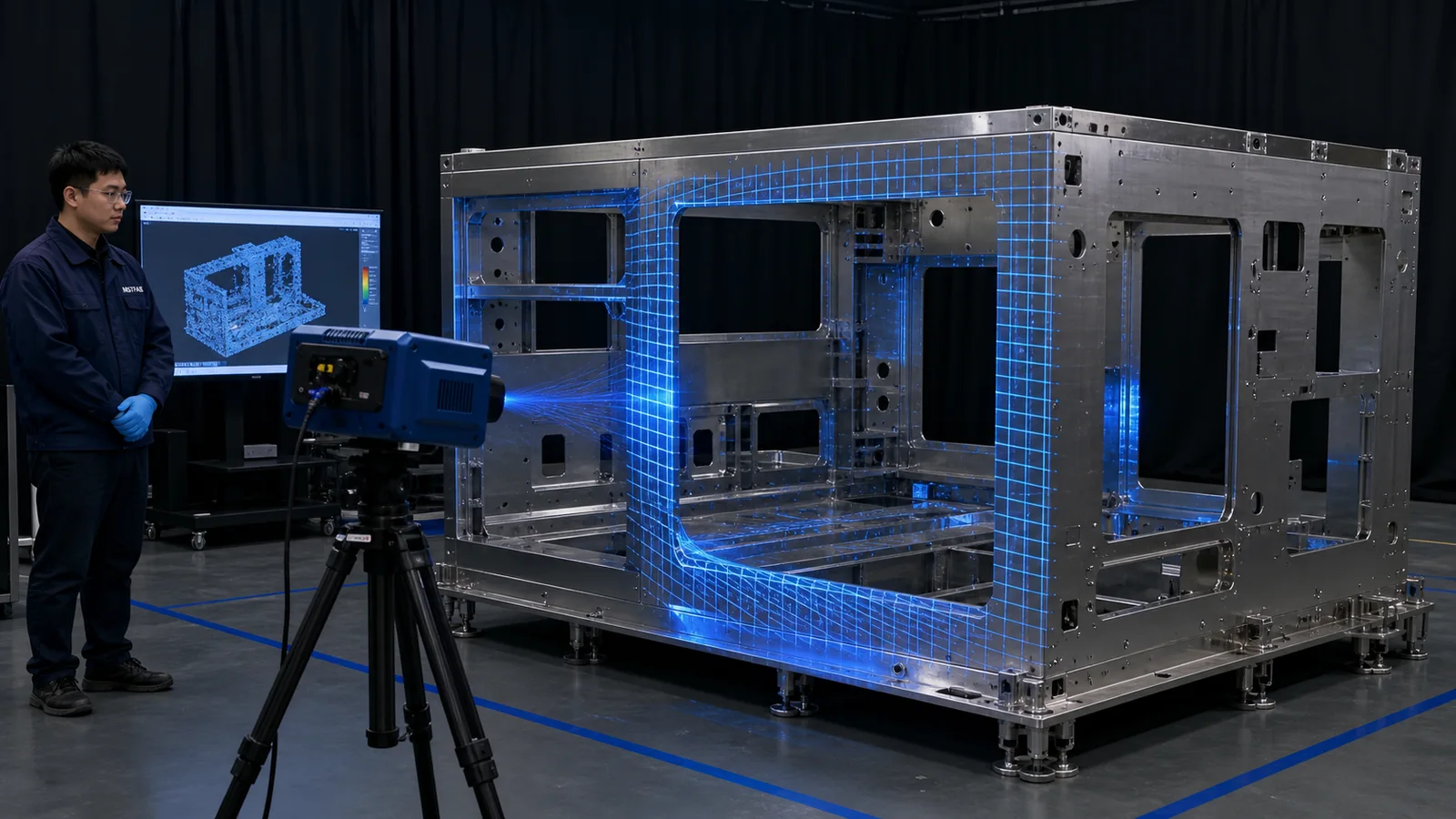
Laser Projection Verification for Multi-Axis Cutouts
Semiconductor tool enclosures contain hundreds of complex interface cutouts for vacuum lines, chemical feedthroughs, optical sensors, and EMO emergency stop buttons. MSTFAB verifies punch patterns using overhead CAD laser projection systems, projecting 1:1 digital cutlines directly onto formed assemblies to ensure zero interference before finishing.
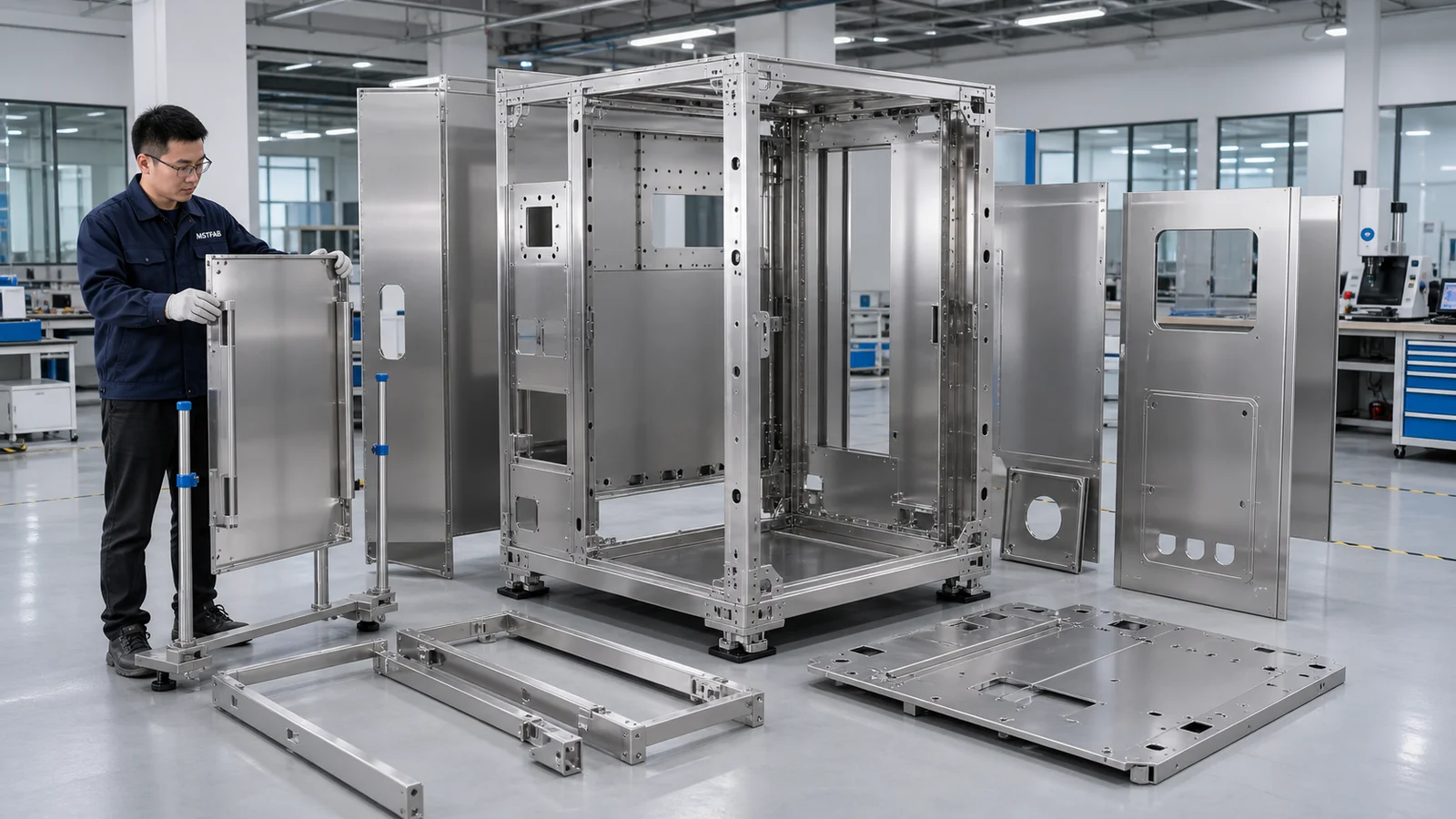
Precision Semiconductor Enclosures Fabricated by MSTFAB
MSTFAB manufactures high-precision semiconductor equipment enclosures, frames, and sub-assemblies. SEMI S2 compliant DFM, ESD powder coating, and clean packaging.
Frequently Asked Questions on Semiconductor Enclosures
What is SEMI S2 compliance in sheet metal enclosure design?
SEMI S2 sets Environmental, Health, and Safety (EHS) guidelines for semiconductor manufacturing equipment. In enclosure fabrication, this mandates fail-safe interlock mounting, physical shielding of rotating or high-voltage components, ergonomic access door clearances, and seismic anchoring bracket design.
How are large semiconductor frames packaged for international ocean shipment?
Large tool frames are secured inside custom isolation cradles equipped with shock-absorbing elastomeric dampers. The entire unit is enclosed in a heat-sealed aluminum foil barrier bag with desiccants to maintain <10% relative humidity throughout ocean transport.
 WeChat Contact
 WhatsApp Me Directly