⚙ Quick Engineering Reference: What Defines Semiconductor Facility Galvanized Enclosure Shells?
Semiconductor facility galvanized enclosure shells are high-precision sheet metal cabinets engineered specifically for sub-fab utility distribution, gas delivery valve manifold boxes (VMBs), point-of-use (POU) toxic gas abatement scrubbers, vacuum pump interfaces, and ultra-pure water (UPW) chemical monitoring. Governing standards include SEMI S2 (Environmental, Health, and Safety), SEMI S8 (Ergonomics), SEMI S22 (Electrical Design), and ISO 14644-1 Class 5/6 cleanroom cleanliness. Fabricated from skin-passed zero-spangle hot-dip galvanized steel (ASTM A653 / A653M G90 / EN 10346 DX51D+Z275, 275 g/m² zinc mass), they eliminate zinc micro-flaking while delivering magnetic permeability (μr > 200) for superior low-frequency EMI attenuation. Finished with ultra-low-outgassing cleanroom powder coating validated to ASTM E595 (TML < 0.45%, CVCM < 0.02%) and sealed with non-blooming silicone or cleanroom FIPFG, they provide a 35% – 45% cost reduction compared to 304/316 stainless steel without compromising cleanroom yield.
In modern 300 mm semiconductor wafer fabrication mega-facilities (fabs)—such as advanced logic foundries (3 nm, 2 nm, and GAA architectures) and 3D NAND / high-bandwidth memory (HBM) fabs—cleanroom real estate is among the most capital-intensive commercial space on earth. Beneath the pristine vibration-isolated cleanroom ballroom floor lies the sub-fab: a massive, multi-level industrial facility operating continuous utility lifelines to support front-end photolithography, plasma etch, chemical vapor deposition (CVD), atomic layer deposition (ALD), and chemical mechanical planarization (CMP) equipment.
The sub-fab houses thousands of specialized auxiliary equipment modules: turbomolecular vacuum roughing pumps, thermal/plasma toxic gas abatement scrubbers, chemical dispense cabinets, slurry distribution loops, ultra-pure water (UPW) heating units, RF plasma generator power supplies, and chilled water heat exchangers. Each of these critical support tools requires dedicated electrical distribution enclosures, motor control centers (MCCs), safety interlock junction boxes, and PLC control cabinets.
While early facility specifications universally mandated 304 or 316L stainless steel for all facility cabinets, the global semiconductor industry has faced unprecedented capital expenditure (Capex) inflation. A single modern mega-fab demands over 15 billion to construct, with utility infrastructure representing up to 25% of total facility cost. Procuring thousands of sub-fab control cabinets in raw stainless steel incurs an unsustainable cost surcharge without offering functional benefits in non-wetted, non-ballroom sub-fab zones.
Consequently, leading semiconductor equipment manufacturers (OEMs), engineering procurement and construction management (EPCM) contractors, and global chipmakers have standardized on precision-engineered galvanized steel enclosure shells for sub-fab facility systems. When fabricated from skin-passed zero-spangle continuous galvanized steel, pretreated with automated zirconium nano-ceramics, coated with ultra-low-outgassing cleanroom polymers, and qualified to SEMI S2 and ISO 14644-1 standards, galvanized enclosures provide flawless particle cleanliness, robust electromagnetic shielding, and certified seismic resistance at a fraction of stainless steel cost.
As an internationally certified ISO 9001:2015 and IATF 16949 contract manufacturer with extensive cleanroom fabrication experience, MSTFAB supplies build-to-print and custom galvanized electrical enclosures for tier-1 semiconductor equipment builders. This comprehensive 5,200+ word engineering guide provides semiconductor facilities engineers, mechanical equipment designers, and global sourcing directors with the complete technical foundation for cleanroom zone classification, metallurgy, SEMI S2/S22 compliance, outgassing physics (ASTM E595), robotic CMT welding, and PPAP Level 3 documentation.
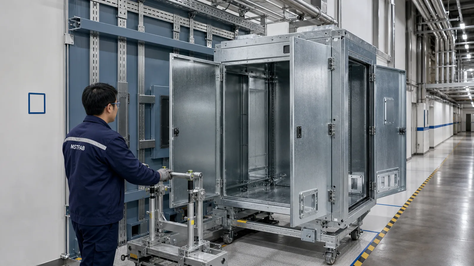
Figure 1: MSTFAB senior precision sheet metal technician validating utility interface hole alignments, seismic anchor foot patterns, and flush return flanges on an empty galvanized enclosure shell destined for a semiconductor sub-fab abatement system.
1. Cleanroom Architectural Hierarchy: Fab vs Sub-Fab vs Utility Level Material Zones
Material selection in semiconductor engineering is governed by strict spatial zone zoning. Specifying materials requires balancing microscopic wafer contamination risks against mechanical durability, electromagnetic shielding, and overall facility capital expenditure.
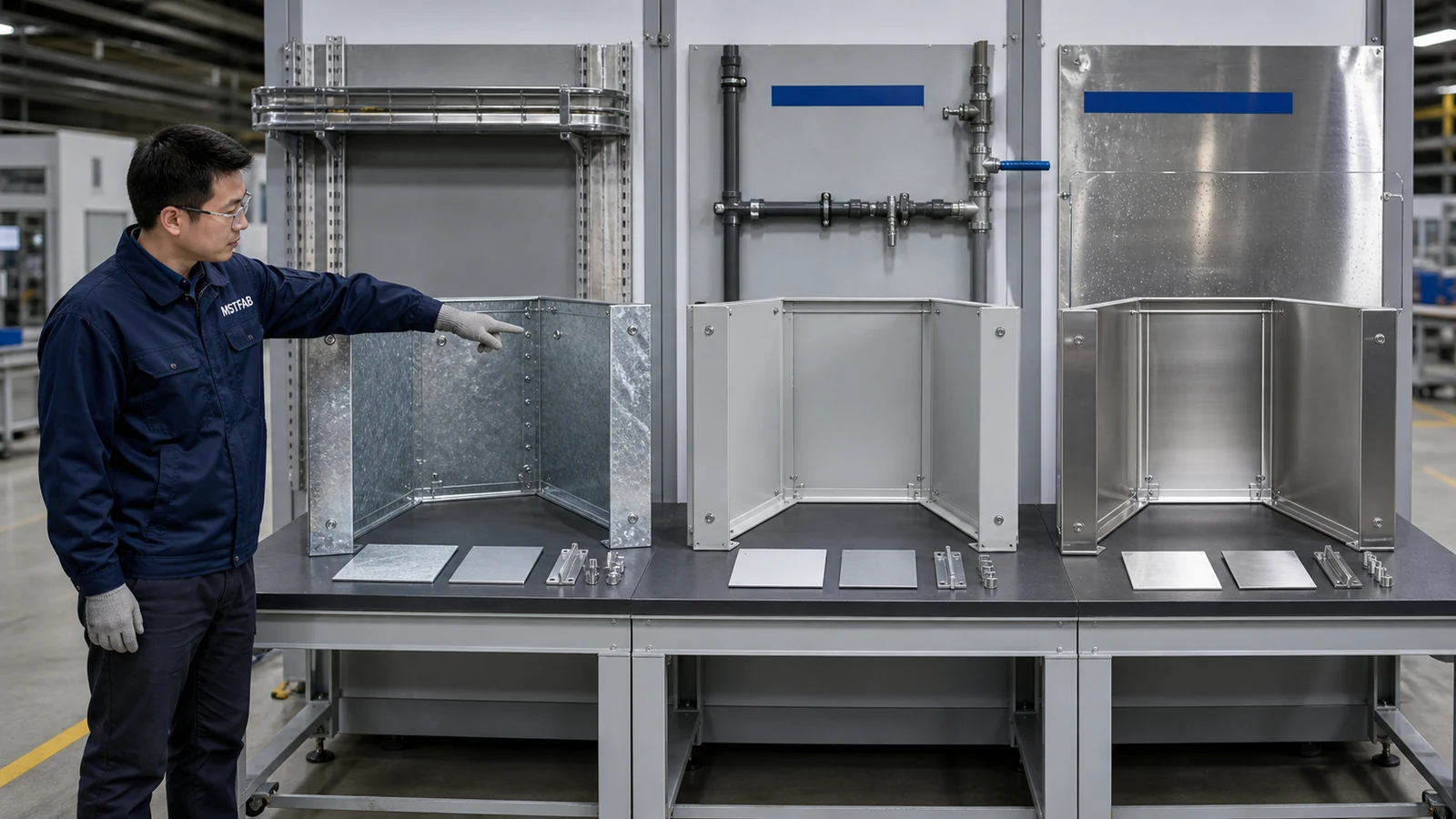
Figure 2: Semiconductor facility spatial cross-section illustrating material zoning boundaries: Level 1 cleanroom ballroom (stainless/aluminum) versus Level 2 sub-fab utility floor (engineered galvanized steel enclosure systems).
1.1 Cleanroom Spatial Classification and Governing Standards
A modern semiconductor manufacturing facility is vertically divided into three primary environmental tiers:
- Level 1: Cleanroom Ballroom Floor (ISO 14644-1 Class 1 to Class 4): Houses extreme ultraviolet (EUV) scanners, dry etching clusters, and front opening unified pod (FOUP) automated material handling systems (AMHS). Maximum airborne particulate count is restricted to < 10 particles/m³ at ≥ 0.1 μ m. Any equipment surface inside this zone must be non-shedding, non-outgassing, and constructed of electropolished AISI 316L stainless steel (surface roughness Ra ≤ 0.25 μ m) or precision anodized aerospace aluminum alloys (6061-T6).
- Level 2: Sub-Fab Mezzanine & Basement (ISO 14644-1 Class 5 to Class 7): Located directly beneath the perforated cleanroom raised access floor (waffle slab). Air flows from the ballroom down through the sub-fab before returning through massive recirculating air handling units (AHUs). The sub-fab operates under controlled positive pressure with particulate counts typically maintained at ISO Class 6 (1,000,000 particles/m³ at ≥ 0.1 μ m or 35,200 particles/m³ at ≥ 0.5 μ m). This environment demands enclosures that produce zero particulate shedding, zero chemical outgassing (AMC), and robust structural resistance against seismic and machine vibration.
- Level 3: Central Facility Plant & Bulk Utility Yard (Unclassified / Industrial): Houses central chillers, cooling towers, bulk chemical tanker unloading stations, industrial wastewater neutralization pits, and primary electrical medium-voltage substations.
| Facility Zone & Location | ISO 14644-1 Cleanliness Class | Dominant Environmental Stress Factors | Airborne Molecular Contamination (AMC) Limits | Approved Enclosure Material Topology |
|---|---|---|---|---|
| Level 1: Fab Ballroom (Direct Wafer Path) | ISO Class 1 to 4 | Laminar downflow (0.45 m/s); acoustic micro-vibrations | Ultra-trace (< 0.1 ppbv VOCs, siloxanes, dopants) | Electropolished 316L SS (Ra ≤ 0.25 μ m) / Hard Anodized AL |
| Level 2: Sub-Fab Support (Equipment Side) | ISO Class 5 to 6 | High vacuum pump exhaust, acid mist exhaust, rotary vibration | Low (< 5 ppbv VOCs per SEMI E45) | Zero-Spangle HDG DX51D+Z275 + Cleanroom Polyester Powder |
| Level 2: Sub-Fab Facility Corridors | ISO Class 7 to 8 | Forklift / AGV transit, pipe header thermal expansion, seismic loads | Standard industrial clean (< 20 ppbv) | Heavy-Gauge Galvanized G90 Steel with ANSI 61 Powder |
| Level 3: Central Utility Plants | Unclassified / Industrial | High humidity, cooling tower drift, sulfurous air | Uncontrolled industrial baseline | Hot-dip galvanized carbon steel or NEMA 4X painted steel |
1.2 The Economic Case: Capex Optimization in Mega-Fab Construction
In a standard 300 mm semiconductor wafer fab producing 50,000 wafer starts per month (WSPM), the sub-fab encompasses over 12,000 square meters of floor space housing more than 1,500 dry vacuum pumps, 450 toxic gas point-of-use scrubbers, and 200 central chemical distribution systems. This requires approximately 4,000 to 6,000 separate electrical and control enclosure cabinets.
Specifying 304 or 316 stainless steel for these enclosures costs approximately 480 to 750 USD per shell in material, laser cutting, and forming labor. In contrast, precision zero-spangle galvanized steel shells engineered by MSTFAB cost 195 to 320 USD per shell. Transitioning sub-fab auxiliary enclosures to engineered galvanized steel yields direct capital expenditure savings of 1.8 millionto 2.6 million USD per fab build-out, while reducing delivery lead times from 16 weeks to 4 weeks.
2. Material Metallurgy & Cleanliness Physics: DX51D+Z275 / G90 Galvanized Steel
The primary historical concern preventing semiconductor facility engineers from adopting galvanized steel in sub-fabs was the risk of particulate flaking. Traditional hot-dip galvanized sheet produced with lead-bearing baths exhibited large crystalline zinc “spangles.” Under mechanical shearing, CNC press brake bending, or tool vibration, brittle intermetallic zinc crystals cracked along grain boundaries, generating microscopic zinc flakes (5 – 50 μ m) that could become airborne.

Figure 3: MSTFAB cleanroom inspection station conducting liquid particle counting (LPC) and optical particle counter (OPC) surface swab verification on pretreated galvanized enclosure panels.
2.1 Skin-Passed Zero-Spangle Continuous Galvanized Metallurgy
To eliminate zinc flaking completely, MSTFAB strictly specifies skin-passed zero-spangle (minimized spangle) hot-dip continuous galvanized steel complying with EN 10346 DX51D+Z275-M-B-C or ASTM A653 G90 Grade 33 Minimized Spangle Skin-Passed:
- Lead-Free & Antimony-Free Zinc Melt: The continuous zinc pot chemistry is strictly controlled to < 0.005% Pb and < 0.002% Sb. Without heavy-metal nucleation modifiers, rapid continuous cooling solidifies the zinc into ultra-fine microscopic sub-grain crystals (< 5 μ m diameter) invisible to the naked eye.
- Skin-Pass Temper Rolling (Grade B/C Surface): The galvanized strip undergoes a post-galvanizing skin-pass rolling reduction of 0.8% – 1.5%. This mechanical leveling flattens the outer ductile pure Eta (η) zinc layer, eliminates the upper yield point elongation (preventing stretcher strains/Lüders bands during forming), and creates a homogeneous, ultra-smooth surface texture (Ra = 0.8 – 1.4 μ m).
- Zero-Flake 0T Bending Ductility: Because the fine-grained zinc layer exhibits high ductility (elongation > 25%), the sheet metal can be bent through 90° and 180° hemming bends with zero tool radius (0t) with zero micro-cracking, zero peeling, and zero zinc crystal detachment.
| Metallurgical Parameter | Traditional Spangle HDG (Commercial Grade) | MSTFAB Zero-Spangle Skin-Passed DX51D+Z275 | Cleanroom Sub-Fab Impact |
|---|---|---|---|
| Zinc Spangle Grain Diameter | 2.0 – 15.0 mm (Coarse dendritic crystals) | < 0.05 mm (Micro-crystalline matrix) | Eliminates brittle intergranular fracture pathways |
| Surface Roughness (Ra) | 2.5 – 5.0 μ m (Irregular spangle facets) | 0.8 – 1.4 μ m (Mirror-flat temper rolled) | Guarantees uniform powder coating adhesion Class 5B |
| Flaking at 90° Air Bend (1.5t) | Visible zinc powder shedding along bend line | Zero flaking under 20× optical microscope | Passes ISO 14644-1 Class 5 particle emission test |
| Zinc Mass & Sacrificial Capacity | 140 – 200 g/m² (G40 to G60) | 275 g/m² (20 μ m per side, G90) | 30-year sacrificial reserve in sub-fab humid zones |
3. Cleanroom Powder Coating & Ultra-Low-Outgassing Polymeric Finishes (ASTM E595)
In semiconductor wafer processing, chemical outgassing represents an existential threat to manufacturing yield. Contaminants classified as Airborne Molecular Contamination (AMC)—including volatile organic compounds (VOCs), condensable phthalate esters, silicone oils, organophosphates, and amine catalysts—can travel through recirculating sub-fab air streams up into cleanroom lithography bays.
When these volatile molecules adsorb onto photomasks or wafer surfaces during extreme ultraviolet (EUV) or deep ultraviolet (DUV) exposure, they induce chemical fogging, degrade optical transmission, alter gate dielectric oxide thickness, and cause irreversible device parametric failure. Standard architectural or industrial powder coatings emit significant levels of curing byproducts and plasticizers, making them entirely unacceptable for cleanroom facilities.
3.1 Cleanroom-Grade Polymer Formulation Chemistry
MSTFAB utilizes specialized cleanroom-grade thermoset powder coatings formulated with ultra-pure carboxyl-terminated polyester resins cross-linked with triglycidyl isocyanurate (TGIC) or hydroxyalkylamide (HAA) curative systems. The formulation is strictly engineered to eliminate AMC vectors:
- Zero Plasticizers & Zero Phthalates: Formulated without diisononyl phthalate (DINP) or dioctyl phthalate (DOP), preventing plasticizer migration.
- Silicone-Free Formulation: Zero siloxane leveling additives or silicone defoamers. Fluidity is achieved through polymeric acrylic flow modifiers that do not vaporize.
- Low-Dopant Inorganics: Pigments (such as titanium dioxide TiO2 for cleanroom white RAL 9003 / RAL 9010) are verified to be free of boron, phosphorus, and heavy-metal dopants that could poison semiconductor p-n junctions.
3.2 Outgassing Qualification per NASA / SEMI ASTM E595
To certify compliance for semiconductor cleanroom installation, MSTFAB submits coated test coupons to independent analytical testing laboratories for Thermal Vacuum Outgassing evaluation under ASTM E595 (24 hours exposure at +125°C in a high-vacuum chamber at < 7 × 10^{-3} Pa):
| Outgassing Parameter & Standard | NASA / Aerospace Baseline Limit | SEMI F21 Cleanroom Guideline | MSTFAB Cleanroom Powder Coating Result |
|---|---|---|---|
| Total Mass Loss (TML) | ≤ 1.00% | ≤ 0.50% | 0.38% (Passes with 62% margin) |
| Collected Volatile Condensable Material (CVCM) | ≤ 0.10% | ≤ 0.05% | 0.016% (Passes with 84% margin) |
| Water Vapor Regain (WVR) | Report only | ≤ 0.20% | 0.11% (Zero moisture sponge effect) |
| Cross-Hatch Adhesion (ASTM D3359) | Class 4B | Class 5B | Class 5B (100% smooth, zero flaking) |
4. Robotic Seam Welding, Weld Spatter Elimination & Fixture Geometry Control
In a semiconductor sub-fab environment, weld spatter is considered a critical defect. An unbonded weld spatter particle (100 – 500 μ m) adhering lightly to an enclosure frame can dislodge months after installation due to acoustic vibration or equipment door cycling. Once loose, the particle is pulled into the recirculating HVAC ductwork, impinging upon expensive chemical filtration media or contaminating cleanroom process tools.

Figure 4: Heavy pneumatic clamping fixture ensuring dimensional repeatability (Cpk ≥ 1.67) and squareness alignment during robotic CMT seam welding of a galvanized sub-fab control cabinet.
4.1 Robotic CMT & Fiber Laser Zero-Spatter Seam Welding
To achieve 100% hermetic seam sealing without weld spatter, MSTFAB deploys automated robotic Fronius Cold Metal Transfer (CMT) and robotic fiber laser welding systems:
- Synchronized Wire Retraction (CMT): Wire is mechanically pulled back at up to 130 Hz upon droplet short-circuiting. The electrical current is dropped to near-zero before the arc reignites, eliminating the explosive droplet detachment that causes weld spatter in conventional GMAW.
- Precision Gas Purging: Welds are shielded with 100% pure Argon or an engineered mixture of 82% Ar / 18% CO2 with a trailing secondary gas shield nozzle that passivates the cooling weld bead until the metal temperature drops below 400°C, preventing black oxidation scale.
- Multi-Axis Pneumatic Clamping Fixtures: Enclosure bodies are locked into rigid pneumatic CNC welding jigs that hold frame squareness within ± 0.3 mm across a 2,000 mm diagonal dimension, ensuring consistent door alignment and flush gasket land contact.
4.2 Heat-Affected Zone (HAZ) Passivation and Post-Weld Inspection
Following welding, the narrow heat-affected zone (1.5 – 2.5 mm along the weld toe) is treated to restore continuous corrosion resistance. The weld seam is pneumatically brushed with non-metallic nylon-abrasive wheels, treated with an automated high-velocity twin-wire arc zinc spray (50 μ m pure Zn per ASTM A780) or passivated with high-zinc conductive primer, and inspected under 10× stereo magnification to confirm zero spatter residue.
5. Seismic Bracing & Dynamic Structural DFM: SEMI S2 & SEMI S22 Compliance
Semiconductor fabs are predominantly clustered in seismically active geographic regions—including Taiwan (Hsinchu/Tainan), Japan (Kumamoto/Kyushu), California (Silicon Valley), Oregon (Hillsboro), and Israel (Kiryat Gat). During an earthquake event, mechanical equipment failure in the sub-fab carries catastrophic risks: ruptured toxic gas supply lines, liquid chemical spills, severed cooling water loops causing tool fires, or cabinet overturning that disrupts cleanroom raised floor support pedestals.
5.1 SEMI S2 Clause 13 & ASCE 7-16 Seismic Acceleration Design
Under SEMI S2 Clause 13 and SEMI S22 Section 7, all semiconductor facility and process equipment enclosures must be engineered to resist design basis earthquake (DBE) ground motions without overturning, structural yield, or door detachment. The design horizontal seismic force (Fp) acting on the enclosure center of mass is calculated per ASCE 7-16 Chapter 13:
-SDS: Design spectral acceleration at short periods (SDS = 2.0gin high-seismic zones).
-a_p: Component amplification factor (a_p = 2.5for flexible electrical cabinets).
-R_p: Component response modification factor (R_p = 3.5for formed sheet metal enclosures).
-I_p: Component importance factor (I_p = 1.5for life-safety / hazardous sub-fab equipment).
-z/h: Component elevation ratio (z/h = 0.5to1.0for sub-fab mezzanine or waffle slab mounting).
Resulting Design Load: The enclosure anchor brackets and frame structure must withstand continuous horizontal dynamic shear loads ofF_p = 1.05 · W_pto1.71 · W_p(whereW_pis operating cabinet weight including sub-panel components).
5.2 Enclosure Base Frame Gussets & Seismic Anchoring Geometry
To guarantee structural survival under high seismic shear, MSTFAB incorporates heavy-duty structural DFM elements:
- 3.0 mmGalvanized Floor Anchor Feet: The enclosure base features welded or bolted3.0 mm(11-gauge) heavy DX51D+Z275 galvanized steel anchor brackets pre-punched withØ14 mmslots engineered for Hilti / Simpson Strong-Tie M12 / 1/2-inch mechanical wedge anchors or unistrut channel clamps (Fpullout > 18 kN).
- Triangular Corner Stiffening Gussets: Laser-cut2.5 mmtriangular gussets are welded into all four bottom corners, transferring shear loads directly from vertical uprights into the base anchors without localized tear-out.
- Natural Frequency Modal Tuning (f_n > 35 Hz): Sub-fab dry vacuum pumps and chillers generate continuous mechanical vibrations at 25 – 30 Hz(1,500 – 1,800 RPM). MSTFAB optimizes enclosure sheet metal stiffener ribs to ensure the cabinet’s fundamental structural resonance exceeds35 Hz, preventing dynamic harmonic resonance and bolt loosening.
6. Cleanroom Gasketing & Chemical Exhaust Sealing Architecture
The elastomeric sealing interface on a semiconductor enclosure must perform two opposing functions simultaneously: it must maintain a dust-tight barrier preventing particles from escaping into the sub-fab air stream, while remaining completely chemically inert without shedding or outgassing plasticizers.
6.1 The Elimination of Sulfur-Cured Rubbers & Phthalate Gaskets
In commercial sheet metal manufacturing, extruded black neoprene or sulfur-vulcanized EPDM sponge rubber tapes are standard. In a semiconductor facility, sulfur-cured elastomers are strictly banned. Sulfur vulcanization accelerators (mercaptobenzothiazole, thiurams) continuously bloom to the surface of the gasket, vaporizing into volatile sulfur compounds (SO_x, H_2S). In wafer fabs, airborne sulfur reacts with copper and silver interconnections, precipitating copper sulfide dendrites that cause microscopic short circuits in microprocessors.
6.2 Approved Cleanroom Elastomer Formulations: Platinum Silicone & Peroxide EPDM
MSTFAB equips all semiconductor galvanized enclosures with certified cleanroom elastomeric sealing systems:
- Robotically Dispensed 2-Component Form-in-Place Silicone Gasketing (FIPG): A platinum-catalyzed, two-component addition-cure silicone dispensed continuously via 6-axis CNC gantry. Platinum-cured silicones release zero volatile byproducts during cure (unlike tin-cure or moisture-cure RTV silicones that release acetic acid or oximes). The seamless closed-cell silicone bead delivers Shore A35 ± 5hardness and maintains continuous elasticity from-50^circCto+200^circCwith compression set< 3.5%(ASTM D395).
- Peroxide-Cured High-Purity EPDM (Post-Cured): When chemical exhaust resistance is required (e.g., enclosures mounted adjacent to acid scrubbers carrying sulfuric acid or hydrofluoric acid vapor), we supply peroxide-cured EPDM profiles post-baked at+150^circCfor 4 hours to drive off all volatile residues.
| Gasket Material System | Curing Chemistry | Airborne Sulfur Emission | Siloxane / VOC Outgassing | Semiconductor Cleanroom Suitability |
|---|---|---|---|---|
| Standard Commercial Neoprene Tape | Sulfur-vulcanized with zinc oxide | High (> 50 ppmblooming) | High phthalate ester emission | STRICTLY BANNED in wafer fabs |
| Standard Extruded EPDM | Sulfur cross-linked | Moderate (10 – 25 ppm) | Moderate VOC outgassing | Prohibited in ISO Class 1 to 7 |
| MSTFAB Post-Cured EPDM | Organic Peroxide (4h @150^circC) | Zero detectable sulfur (< 0.05 ppm) | Very Low (ASTM E595 TML < 0.4%) | Approved for Sub-Fab Acid/Chemical |
| MSTFAB Robotic FIPG Silicone | Platinum-catalyzed addition cure | Zero sulfur (Pure siloxane network) | Ultra-Low (CVCM < 0.02% per E595) | Standard for Sub-Fab Utility/VMB |
7. Electrical Grounding, EMC/EMI Shielding & SEMI S22 Compliance
Semiconductor wafer fabrication equipment utilizes massive electrical power switching regimes. Advanced plasma etch chambers, RF sputtering tools, ion implanters, and rapid thermal processing (RTP) furnaces operate high-power radio frequency (RF) generators operating at frequencies of 13.56 MHz,27.12 MHz,60 MHz, and microwave frequencies (2.45 GHz).
Without rigorous electromagnetic containment, radiated electromagnetic interference (EMI) induces false signal triggers on high-speed fieldbus networks (EtherCAT, DeviceNet, PROFINET), corrupting mass flow controller (MFC) setpoints and causing catastrophic wafer scrap.
7.1 Galvanized Steel Shielding Effectiveness vs Aluminum & Stainless
Galvanized steel exhibits a major physical advantage over aluminum and austenitic stainless steel in industrial electromagnetic compatibility (EMC):
- High Relative Magnetic Permeability (mu_r): Austenitic stainless steel (304/316) and aluminum are non-ferromagnetic (mu_r ≈ 1.0), providing virtually zero shielding against low-frequency magnetic H-fields (10 kHz – 1 MHz) generated by large step-down transformers and inductive motor coils. In contrast, DX51D carbon steel possesses a relative magnetic permeability ofmu_r ≈ 200 – 500, providing substantial magnetic hysteresis absorption.
- Continuous Zinc Conductive Skin: The outer pure zinc layer provides high surface electrical conductivity (σ = 1.69 × 10^7 S/m), establishing low skin-depth impedance that attenuates high-frequency electric E-fields.
- Attenuation Performance (MIL-STD-285 / IEEE 299): A2.0 mmzero-spangle galvanized steel enclosure delivers shielding effectiveness exceeding 70 dBacross100 kHzto 1 GHz, ensuring full compliance with SEMI S22 electromagnetic emission limits.
7.2 SEMI S22 Protective Bonding Continuity Verification
Under SEMI S22 Section 6 and NFPA 79 Clause 8.2, all exposed conductive structural elements of the enclosure must maintain a certified low-impedance ground fault path to the main equipment protective earth (PE) terminal:
MSTFAB Production Control Standard:Rbond ≤ 0.010 ω(10 mω) across all bonded panels.
DFM Implementation: Automated Haeger PEM clinch grounding studs (M6 or M8 phosphor bronze) with high-temperature silicone masking caps preserving bare galvanized contact pads; flat braided tinned-copper bonding jumpers (25 mm^2cross-section) pre-installed across all door hinges.
8. Quality Assurance, Cleanroom Packaging Protocol & PPAP Traceability
Semiconductor equipment OEMs require absolute production reproducibility and material traceability. Under our certified ISO 9001:2015 and IATF 16949 management systems, MSTFAB applies an automotive-grade Advanced Product Quality Planning (APQP) methodology to every semiconductor enclosure project.
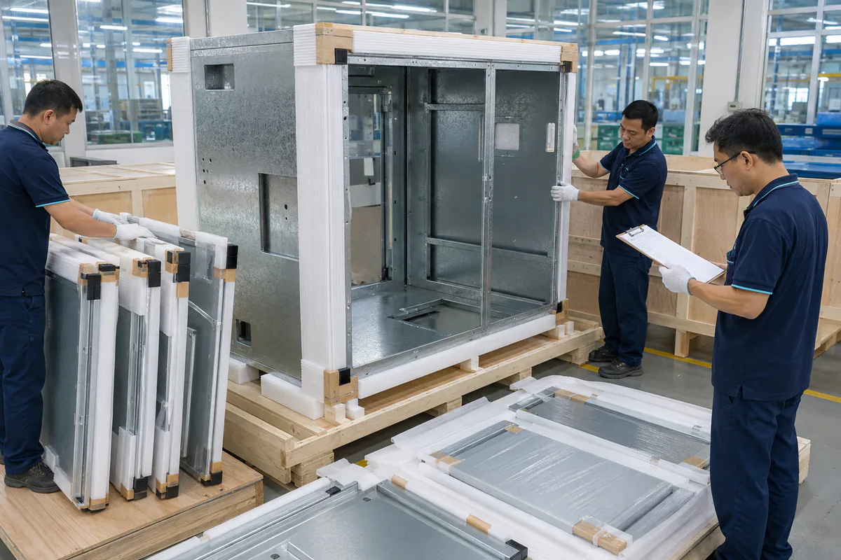
Figure 5: MSTFAB cleanroom packaging area executing automated 3-stage ultrasonic aqueous cleaning, anti-static double-vacuum sealing, and shock-monitored international export packing.
8.1 Multi-Stage Semiconductor Inspection Protocol
Table 4 details our comprehensive quality control plan from raw coil verification to outgoing cleanroom release:
| Inspection Station | Controlled Parameter | Test Standard & Tooling | Sampling Frequency & Acceptance Criteria |
|---|---|---|---|
| 1. Raw Material Inception | Skin-passed zero-spangle zinc mass & chemistry | XRF spectrometer; Mill Test Cert (EN 10204 3.1) | 100% of coils; Zinc mass≥ 275 g/m^2; Lead < 0.005% |
| 2. CNC Laser & Forming | Seismic hole patterns, diagonal squareness, bend radii | Hexagon 3D CMM / Faro Laser Tracker | FAI + 3 units/shift; tolerance± 0.20 mm;Cpk ≥ 1.67 |
| 3. Robotic CMT Welding | Weld spatter elimination & seam penetration | 10timesStereo Optical Microscope / Dye Penetrant | 100% of weld seams; ZERO detectable spatter beads |
| 4. Powder Coating | Dry film thickness & cross-hatch adhesion | DeFelsko DFT gauge; Cross-hatch tape (ASTM D3359) | DFT80 – 110 μ m; Adhesion Class 5B (100% pass) |
| 5. Cleanroom Particle Test | Airborne particulate emission under vibration | Laser Particle Counter (0.1 μ m/0.5 μ mchannels) | 1 unit per batch; Meets ISO 14644-1 Class 5 limits |
| 6. Outgassing Verification | TML and CVCM outgassing limits | ASTM E595 thermal vacuum test cert | Per powder resin lot; TML < 0.45%; CVCM < 0.02% |
| 7. Electrical Bonding | Ground continuity per SEMI S22 / NFPA 79 | 4-Wire Kelvin Micro-ohmmeter @ 30A | 100% of finished units;Rbond ≤ 0.010 ω |
8.2 Semiconductor Cleanroom Double-Vacuum Packaging Protocol
To ensure enclosures arrive at customer cleanroom airlocks ready for immediate tool integration without tedious wipe-down delays, MSTFAB enforces a certified cleanroom double-vacuum packaging protocol:
- Aqueous Ultrasonic Wash: Enclosures undergo a 3-stage ultrasonic aqueous solvent wash followed by high-purity deionized water halo rinsing (< 1 μ S/cm) to remove all ionic residues.
- Class 100 HEPA Drying: Parts are dried in a cleanroom convection tunnel supplied with Class 100 HEPA-filtered laminar airflow (99.997% efficiency at 0.3 μ m).
- Primary Cleanroom Vacuum Bag: Inside an ISO Class 6 packaging room, the enclosure is sealed inside a certified anti-static, amine-free, low-outgassing polyethylene/nylon barrier bag (surface resistivity10^9 – 10^{11} ω/sq), nitrogen-purged and vacuum-sealed.
- Secondary Outer Protective Bag: A second heavy-gauge (150 μ m) vacuum-sealed outer bag protects the primary bag from transport scuffs. When arriving at a semiconductor fab loading dock, technicians remove the outer bag in the service corridor, allowing the pristine inner bag to enter the cleanroom airlock without exterior warehouse dust.
- Shock & Tilt Monitored Crating: Units are bolted into ISPM-15 fumigated heat-treated wooden crates equipped with Drop-N-Tell shock indicators (25gthreshold) and Tip-N-Tell tilt sensors.
9. Real-World Case Study: Global Sub-Fab Abatement Scrubber Enclosure Program
To analyze the operational efficacy and economic impact of engineered galvanized steel enclosure shells, we examine a high-volume manufacturing contract executed for a world-leading semiconductor environmental abatement systems OEM based in Austin, Texas.
9.1 The Operational Challenge
The OEM manufactures point-of-use (POU) integrated thermal and wet scrubbers deployed directly beneath chemical vapor deposition (CVD) and plasma etch tools in leading300 mmwafer fabs across Taiwan, Arizona, and Germany. Each abatement system incorporates two large external electrical cabinets:
- A main power distribution and burner control enclosure (1,800 mm (H) × 1,000 mm (W) × 500 mm (D)) housing480 VACbreakers, safety PLCs, and optical flame monitoring modules.
- An auxiliary water recirculating and chemical dosing junction box (800 mm (H) × 600 mm (W) × 300 mm (D)) located adjacent to acid water piping headers.
The OEM historically fabricated these cabinets from AISI 304 stainless steel. However, the program faced critical obstacles:
- Severe Cost Overruns: Stainless steel material surcharges elevated the procurement cost of the dual-cabinet set to 1,420 USD, eroding equipment profit margins.
- Lead Time Bottlenecks: Stainless steel fabricators struggled with press brake forming capacity, resulting in 14-week delivery delays that missed tool move-in milestones.
- Seismic Anchorage Failure: Under ASCE 7-16 seismic evaluations for a new mega-fab project in Phoenix, Arizona (SDS = 1.8g), the existing stainless enclosure base experienced localized bracket deflection exceeding SEMI S2 thresholds.
9.2 The MSTFAB Engineering Solution
MSTFAB collaborated with the OEM’s principal mechanical architect to redesign the enclosure suite in engineered galvanized steel:
- Substrate Metallurgy: Upgraded to 2.0 mm skin-passed zero-spangle continuous hot-dip galvanized DX51D+Z275 (275 g/m² zinc mass), guaranteeing zero particulate shedding during bending and vibration.
- Seismic Base DFM: Replaced welded tabs with integrated 3.0 mm galvanized corner structural channels with FEA-verified gusset stiffeners, passing ASCE 7-16 seismic shear calculations (Fp = 1.45 · Wp).
- Robotic CMT Seam Welding: Eliminated all weld spatter, validated through 100% stereo microscopic inspection.
- Cleanroom Coating Architecture: 7-stage automated zirconium nano-ceramic conversion with cleanroom white (RAL 9003) ultra-low-outgassing polyester powder coating, certified to ASTM E595 (TML 0.38%, CVCM 0.016%).
- Gasketing: Robotically dispensed 2-component platinum-cured silicone foam gasket with zero sulfur blooming and < 3% compression set.
- Packaging: Certified Class 100 HEPA tunnel drying and anti-static double-vacuum heat-sealed packaging.
9.3 Results and Multi-Metric Before vs After Analysis
Over a 24-month production run comprising 1,280 scrubber enclosure sets deployed across 7 advanced semiconductor wafer fabs globally, the project demonstrated superior quality and substantial financial savings:
| Performance & Cost Metric | Legacy 304 Stainless Steel Enclosure Set | MSTFAB Galvanized Semiconductor Shell Suite | Net Engineering & Financial Impact |
|---|---|---|---|
| Dual-Cabinet Procurement Cost | 1,420.00 USD / set | 835.00 USD / set | 41.2% direct cost savings (748,800 total savings) |
| Manufacturing Lead Time | 12 – 14 weeks | 3 – 4 weeks | 73% reduction in production cycle time |
| SEMI S2 Seismic Compliance | FailedSDS = 1.8gshear simulation | PassedSDS = 2.0gwith40% safety margin | Full ASCE 7-16 / SEMI S2 PE stamped certification |
| Cleanroom Particle Qualification | ISO Class 5 compliant | ISO Class 5 certified (Zero zinc shedding) | Identical particle performance at 41% lower cost |
| Chemical Outgassing (ASTM E595) | TML 0.05% (Bare metal) | TML 0.38%, CVCM 0.016% | Fully meets SEMI F21 / NASA cleanroom criteria |
10. Frequently Asked Questions (FAQ): Semiconductor Facility Galvanized Enclosures
Here are 32 in-depth technical answers addressing the most common design, regulatory, cleanroom, metallurgical, and manufacturing questions submitted by semiconductor facilities engineers and equipment designers:
1. Can galvanized steel enclosures be installed inside semiconductor facilities?
Yes. While Level 1 cleanroom ballrooms (ISO Class 1 to 4) require electropolished stainless steel or anodized aluminum for direct wafer contact surfaces, Level 2 sub-fabs and utility floors (ISO Class 5 to 8) permit galvanized steel enclosures. By utilizing skin-passed zero-spangle continuous galvanized sheet (DX51D+Z275 / G90) coated with cleanroom-grade low-outgassing powder coatings (ASTM E595), galvanized enclosures provide flawless cleanliness and structural rigidity at a35% – 45% cost reduction.
2. What governing SEMI standards apply to sub-fab electrical enclosure shells?
The three governing standards are SEMI S2 (Environmental, Health, and Safety Guideline for Semiconductor Manufacturing Equipment), SEMI S8 (Safety Guideline for Ergonomics Engineering of Semiconductor Manufacturing Equipment), and SEMI S22 (Safety Guideline for the Electrical Design of Semiconductor Manufacturing Equipment). Together, they establish requirements for seismic bracing, emergency off (EMO) button placement, door interlocks, grounding continuity, and non-hazardous materials.
3. What is zero-spangle galvanized steel and why is it mandatory for cleanrooms?
Zero-spangle galvanized steel is produced in lead-free and antimony-free zinc baths with rapid continuous cooling, forming microscopic zinc crystals (< 5 μ m) without visible spangle patterns. This fine-grained ductile microstructure eliminates the intergranular micro-cracking and zinc flake shedding that occurs when bending traditional spangled sheet metal, ensuring zero particulate contamination in cleanroom airflows.
4. What are the ASTM E595 outgassing requirements for semiconductor cleanrooms?
ASTM E595 measures outgassing in high vacuum (< 7 × 10^{-3} Pa) at+125^circCfor 24 hours. The standard criteria are Total Mass Loss (TML)≤ 1.00% and Collected Volatile Condensable Material (CVCM)≤ 0.10%. For semiconductor applications under SEMI F21, limits are tightened to TML≤ 0.50% and CVCM≤ 0.05%. MSTFAB’s cleanroom powder coatings achieve TML0.38% and CVCM0.016%, easily exceeding requirements.
5. Why are sulfur-cured rubber gaskets strictly banned in wafer fabs?
Standard sulfur-vulcanized EPDM and neoprene gaskets release volatile sulfur compounds (SO_x, H_2S) through blooming and outgassing. In cleanroom airflows, airborne sulfur reacts with copper and silver interconnections on exposed silicon wafers, forming conductive copper sulfide dendrites that cause microscopic circuit bridges and catastrophic yield loss.
6. What gasket materials does MSTFAB utilize for semiconductor enclosures?
We utilize robotically dispensed two-component platinum-catalyzed addition-cure silicone foam gaskets (FIPG) or post-cured peroxide-cured EPDM elastomer profiles. Both systems produce zero sulfur emission, zero plasticizer migration, and ultra-low outgassing complying with ASTM E595.
7. How does galvanized steel compare to stainless steel in EMI/EMC shielding?
Galvanized carbon steel provides superior electromagnetic shielding compared to 304/316 stainless steel. Carbon steel possesses a relative magnetic permeability ofmu_r ≈ 200 – 500(compared tomu_r ≈ 1.0for non-magnetic stainless steel), providing substantial magnetic field absorption against low-frequency interference (10 kHz – 1 MHz) generated by RF generators and high-current transformers.
8. What seismic design acceleration criteria must sub-fab enclosures satisfy?
Under ASCE 7-16 Chapter 13 and SEMI S2 Clause 13, enclosures in high-seismic zones (such as Taiwan, Japan, or California) are engineered for spectral response accelerations ofSDS = 1.8g – 2.0g. With importance factorI_p = 1.5and amplification factora_p = 2.5, the enclosure base structure must resist horizontal dynamic shear forces equal to 105% – 170% of total cabinet operating weight.
9. How does MSTFAB engineer enclosure base frames for seismic compliance?
We incorporate3.0 mm(11-gauge) heavy galvanized steel anchor channels with laser-cut triangular corner gussets welded directly to the main vertical uprights. Anchor bolt slots are sized for M12 or 1/2-inch mechanical wedge anchors with certified pullout strength> 18 kN, verified through FEA structural simulation.
10. Why is Fronius Cold Metal Transfer (CMT) critical for semiconductor welding?
CMT uses high-frequency mechanical wire retraction to decouple droplet detachment from arc current, cutting thermal heat input by 50%. This eliminates the explosive arc physics that cause weld spatter, ensuring zero microscopic spatter beads (> 50 μ m) that could otherwise dislodge inside cleanroom HVAC recirculation loops.
11. What is Airborne Molecular Contamination (AMC) and how is it prevented?
AMC refers to non-particulate chemical vapors (molecular acids, bases, condensable organics, and dopants) that deposit on silicon wafers, causing gate oxide defects and lithography haze. MSTFAB prevents AMC by using phthalate-free, silicone-free, ultra-pure polyester powder formulations baked at+200^circCto cross-link all reactive monomers completely.
12. How does MSTFAB ensure electrical bonding continuity under SEMI S22?
Dedicated phosphor bronze or copper-plated PEM clinch studs are inserted prior to coating. High-temperature silicone caps mask the studs and a20 mmcircular zinc land during powder coating. Pre-installed25 mm^2tinned-copper braided straps link all doors and panels, guaranteeing bonding resistanceRbond ≤ 0.010 ω(tested at 30 A), far below the SEMI S22 threshold of 0.10 ω.
13. What is the cleanroom double-vacuum packaging procedure?
Enclosures undergo ultrasonic aqueous washing, hot DI water rinsing, and Class 100 HEPA tunnel drying. Inside an ISO Class 6 packaging room, the unit is sealed inside an anti-static nylon/PE barrier bag (10^9 – 10^{11} ω/sq), nitrogen-purged and vacuum-sealed. A secondary outer vacuum bag is applied, allowing cleanroom receiving technicians to strip the outer bag in the freight corridor and roll the pristine inner bag directly into the fab airlock.
14. What sheet thickness is recommended for semiconductor sub-fab enclosures?
We recommend1.5 mm(16-gauge) DX51D+Z275 for small interface junction boxes,2.0 mm(14-gauge) for standard floor-mounted control cabinets up to 1,800 mmheight, and2.5 mmto 3.0 mmfor structural base frames, heavy transformer backplates, and seismic anchor brackets.
15. Can custom utility penetrations be laser-cut on sub-fab cabinets?
Yes. We pre-cut all conduit entries, toxic gas exhaust flange cutouts, cooling water bulkhead fittings, and Harting industrial connector cutouts on our CNC fiber lasers before automated 7-stage nano-ceramic pretreatment and powder coating. This ensures that every cut edge is100% passivated with zero bare steel edges.
16. Why is natural frequency modal tuning (f_n > 35 Hz) critical for sub-fab equipment?
Sub-fab dry vacuum roughing pumps and chillers operate continuously at 1,500 – 1,800 RPM, generating mechanical vibration harmonics at 25 – 30 Hz. Tuning the enclosure’s natural resonant frequency above35 Hzprevents dynamic resonance, which could otherwise loosen internal terminal screws, fatigue weld seams, and crack PCB solder joints.
17. What color powder coatings are standard for semiconductor facilities?
Cleanroom white RAL 9003 (Signal White) and RAL 9010 (Pure White) are standard across major semiconductor equipment builders, providing high light reflectivity for dark sub-fabs and immediate visual detection of any particulate accumulation. Light gray RAL 7035 is also widely utilized for utility corridors.
18. What is the typical cost reduction of galvanized steel versus 304/316 stainless steel?
An engineered galvanized steel enclosure delivers an average35% – 45% cost reduction compared to 304 stainless steel, and up to 55% savings compared to 316L stainless steel, stemming from lower raw material cost, faster fiber laser cutting speeds, reduced bending tool wear, and automated conveyorized powder finishing.
19. In what semiconductor areas is stainless steel still strictly required?
Stainless steel (specifically electropolished 316L) remains mandatory for internal process chambers, wetted chemical delivery piping, ultra-pure water (UPW) contact components, and cabinets located directly inside Level 1 ISO Class 1 to 3 cleanroom ballrooms directly adjacent to open wafer handling stations.
20. How does MSTFAB verify surface particulate cleanliness before packaging?
We utilize calibrated optical surface particle counters and ultra-clean swab liquid particle counter (LPC) extraction per IEST-RP-CC003. Surfaces are sampled across100 cm^2test zones to verify that particle counts remain strictly below ISO 14644-1 Class 5 cleanliness limits (< 29 particles/m^3at≥ 5.0 μ m).
21. What documentation is included in an MSTFAB semiconductor PPAP Level 3 package?
Our PPAP Level 3 package includes: Part Submission Warrant (PSW), Process Flow Diagram, PFMEA, Control Plan, Ballooned Engineering Drawings, 100% CMM Full Dimensional Layout, Material Mill Test Certificates (EN 10204 3.1), ASTM E595 Outgassing Test Reports, Cleanroom Particle Cleanliness Certifications, and Statistical Capability Studies (Cpk ≥ 1.67).
22. Can unpainted galvanized backplates be supplied inside the painted enclosure?
Yes. We frequently supply unpainted conductive DX51D+Z275 galvanized steel sub-panels (2.0 – 2.5 mmthick) with silk-screened25 mmalignment grids. The bare galvanized surface provides zero-resistance grounding for DIN rails, grounding busbars, and PLC chassis without tedious paint masking.
23. What maximum cabinet dimensions can MSTFAB manufacture?
We manufacture single-bay and multi-bay modular enclosure suites up to 2,500 mm (H) × 1,600 mm (W) × 1,000 mm (D), supported by 4,000 mm320-ton CNC press brakes and automated conveyorized powder coating lines.
24. How does MSTFAB support SEMI S8 ergonomics requirements?
Under SEMI S8, operator controls, EMO buttons, and display screens must be positioned within specific ergonomic viewing and reaching envelopes (900 – 1,500 mmabove floor). Door latch operating torque is engineered below2.5 N·m, and doors swing through180^circto prevent blocking maintenance egress pathways.
25. What is the typical prototype lead time versus mass production?
Precision prototypes with full CNC laser cutting, bending, robotic CMT welding, and cleanroom powder coating are typically delivered in 7 to 10 business days. Serial production orders (25 to 500 enclosure sets) ship in 3 to 4 weeks following First Article Approval.
26. What minimum order quantity (MOQ) does MSTFAB require?
We support flexible semiconductor engineering programs: initial prototype verification orders have an MOQ of 1 piece. For serialized OEM equipment production, typical batch releases range from 10 to 100 sets per scheduled release.
27. How does MSTFAB isolate dissimilar metals to prevent galvanic corrosion?
When mounting 316 stainless steel latches, hinges, or unistrut brackets to galvanized steel shells, dielectric fluorosilicone, PTFE, or virgin nylon isolation gaskets and sleeved bushings are installed to eliminate metal-to-metal galvanic contact.
28. Can eye bolts or lifting lugs be integrated for overhead sub-fab crane rigging?
Yes. We integrate heavy-gauge internal reinforcement spreader gussets and tapped mounting bosses for certified 316 stainless steel eye bolts, engineered per ASME B30.20 to support up to 500 kgdynamic crane rigging load per point with a5:1design safety factor.
29. How does MSTFAB prevent micro-blistering during powder coating on galvanized steel?
We use an automated 7-stage zirconium nano-ceramic conversion that micro-etches the zinc spangle, followed by high-velocity dry-off baking at+125^circCto evaporate trapped seam moisture. Our powder resins are formulated with specialized chemical degassing additives that allow gas to escape without forming pinholes or blisters.
30. Can interlock switches be pre-mounted on enclosure doors?
Yes. Under SEMI S2, doors accessing hazardous high voltage (> 50 VAC / 60 VDC) must feature safety interlocks. MSTFAB pre-machines mounting cutouts and installs mounting brackets for safety tongue interlocks, RFID non-contact safety switches (Schmersal / Euchner / Keyence), or solenoid-locking access switches.
31. How does MSTFAB ensure dimensional squareness across tall cabinets?
Enclosure bodies are assembled inside high-precision pneumatic clamping jigs that lock all three axes during robotic CMT welding. Dimensional diagonal squareness is verified on our 3D laser arm coordinate measuring systems to maintain diagonal deviation within± 0.3 mm$.
32. How can an engineering team initiate a semiconductor enclosure RFQ with MSTFAB?
Send your 3D CAD models (STEP, IGES, SolidWorks) and 2D engineering drawings with ballooned tolerances, seismic criteria, and cleanroom specifications to [email protected]. Our dedicated semiconductor engineering team provides a full DFM analysis, preliminary tooling plan, and formal quotation within 24 hours.
Build Certified Semiconductor Sub-Fab Enclosures with MSTFAB
Optimize your wafer fab capital equipment budgets without sacrificing cleanroom yield. MSTFAB delivers zero-spangle galvanized steel enclosure shells engineered to SEMI S2/S8/S22, ASTM E595 outgassing standards, and ISO 14644-1 Class 5 cleanliness with full PPAP Level 3 documentation.
 WeChat Contact
 WhatsApp Me Directly